🔀 Logic Gates & Boolean Algebra
AND, OR, NOT, NAND, NOR, XOR, XNOR logic gates with truth tables, Boolean algebra basics, and their role in digital circuits for UPSSSC AGTA.
What are Logic Gates?
Logic gates are the building blocks of every digital circuit inside a computer. They are tiny electronic circuits that take one or more binary inputs (0 or 1) and produce a single binary output based on a specific logical rule.
Every operation a computer performs — from adding numbers to displaying images — is built from combinations of these simple gates. Your CPU contains billions of logic gates working together.
Gate symbols — NAND (amber) is a Universal Gate
The 7 Basic Logic Gates
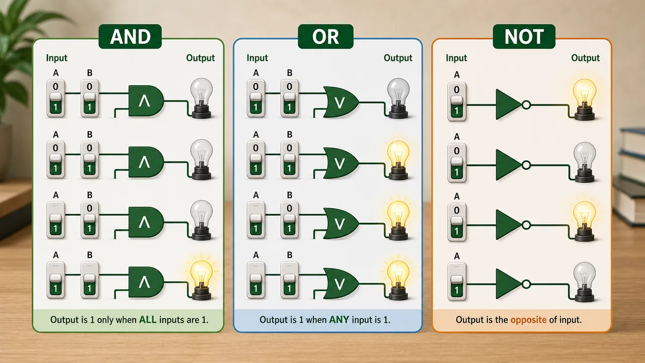
1. AND Gate
The AND gate outputs 1 only when ALL inputs are 1. Think of it as: "Both conditions must be true."
Symbol: A · B (or AB)
| A | B | Output (A·B) |
|---|---|---|
| 0 | 0 | 0 |
| 0 | 1 | 0 |
| 1 | 0 | 0 |
| 1 | 1 | 1 |
Real-life analogy: A car starts only when BOTH the key is inserted AND the brake is pressed. Both conditions must be true.
2. OR Gate
The OR gate outputs 1 when ANY input is 1. Think of it as: "At least one condition must be true."
Symbol: A + B
| A | B | Output (A+B) |
|---|---|---|
| 0 | 0 | 0 |
| 0 | 1 | 1 |
| 1 | 0 | 1 |
| 1 | 1 | 1 |
Real-life analogy: A room light turns on if Switch A OR Switch B (or both) are pressed.
3. NOT Gate (Inverter)
The NOT gate has only one input and it reverses (inverts) it. If input is 1, output is 0. If input is 0, output is 1. Also called an Inverter.
Symbol: Ā (A bar) or A'
| A | Output (Ā) |
|---|---|
| 0 | 1 |
| 1 | 0 |
Real-life analogy: A "Do Not Disturb" sign — when it's ON, entry is OFF; when it's OFF, entry is ON.
4. NAND Gate (NOT + AND)
The NAND gate is the opposite of AND. It outputs 0 only when ALL inputs are 1. Otherwise, it outputs 1.
Symbol: (A·B)' or AB with a bar
| A | B | Output |
|---|---|---|
| 0 | 0 | 1 |
| 0 | 1 | 1 |
| 1 | 0 | 1 |
| 1 | 1 | 0 |
NAND is called a "Universal Gate" because any other gate (AND, OR, NOT) can be built using only NAND gates.
5. NOR Gate (NOT + OR)
The NOR gate is the opposite of OR. It outputs 1 only when ALL inputs are 0. If any input is 1, output is 0.
Symbol: (A+B)' or A+B with a bar
| A | B | Output |
|---|---|---|
| 0 | 0 | 1 |
| 0 | 1 | 0 |
| 1 | 0 | 0 |
| 1 | 1 | 0 |
NOR is also a "Universal Gate" — any gate can be built using only NOR gates.
6. XOR Gate (Exclusive OR)
The XOR gate outputs 1 when inputs are DIFFERENT. If both inputs are the same (both 0 or both 1), output is 0.
Symbol: A ⊕ B
| A | B | Output (A⊕B) |
|---|---|---|
| 0 | 0 | 0 |
| 0 | 1 | 1 |
| 1 | 0 | 1 |
| 1 | 1 | 0 |
Used in: Binary addition (half adder, full adder circuits), error detection, parity checking.
7. XNOR Gate (Exclusive NOR)
The XNOR gate is the opposite of XOR. It outputs 1 when inputs are SAME.
Symbol: A ⊙ B
| A | B | Output |
|---|---|---|
| 0 | 0 | 1 |
| 0 | 1 | 0 |
| 1 | 0 | 0 |
| 1 | 1 | 1 |
Used in: Equality comparison — checking if two values are the same.
Quick Comparison Table
| Gate | Inputs | Output = 1 When | Universal? |
|---|---|---|---|
| AND | 2+ | ALL inputs are 1 | No |
| OR | 2+ | ANY input is 1 | No |
| NOT | 1 | Input is 0 (inverts) | No |
| NAND | 2+ | NOT all inputs are 1 | Yes |
| NOR | 2+ | ALL inputs are 0 | Yes |
| XOR | 2 | Inputs are DIFFERENT | No |
| XNOR | 2 | Inputs are SAME | No |
Boolean Algebra Basics
Boolean algebra is the mathematics of logic gates, using only two values: 0 (False) and 1 (True). It was developed by George Boole in the 19th century.
Basic Laws
| Law | AND Form | OR Form |
|---|---|---|
| Identity | A · 1 = A | A + 0 = A |
| Null | A · 0 = 0 | A + 1 = 1 |
| Complement | A · Ā = 0 | A + Ā = 1 |
| Idempotent | A · A = A | A + A = A |
| Double Negation | (Ā)' = A | (Ā)' = A |
De Morgan's Theorems
Two important theorems for simplifying logic circuits:
- (A · B)' = Ā + B̄ — NOT of AND = OR of NOTs
- (A + B)' = Ā · B̄ — NOT of OR = AND of NOTs
These theorems prove why NAND and NOR are universal gates — they can create any other gate.
Why NAND & NOR are Universal Gates
NAND and NOR are called Universal Gates because any other logic gate can be constructed using only NAND gates (or only NOR gates):
| Gate to Build | Using NAND Only | Using NOR Only |
|---|---|---|
| NOT | Connect both inputs of NAND together | Connect both inputs of NOR together |
| AND | NAND followed by NOT (another NAND) | Three NOR gates |
| OR | NOT each input, then NAND | NOR followed by NOT (another NOR) |
This is why NAND gates are the most commonly used gates in IC (Integrated Circuit) design — entire processors can be built from NAND gates alone.
Boolean Algebra — Additional Laws
| Law | Expression | Meaning |
|---|---|---|
| Commutative | A + B = B + A; A · B = B · A | Order does not matter |
| Associative | (A+B)+C = A+(B+C); (A·B)·C = A·(B·C) | Grouping does not matter |
| Distributive | A·(B+C) = A·B + A·C | Multiply over addition |
| Absorption | A + A·B = A; A·(A+B) = A | Simplification rule |
De Morgan's Theorems (Restated Clearly)
- Theorem 1: NOT(A AND B) = NOT A OR NOT B → (A·B)' = A' + B'
- Theorem 2: NOT(A OR B) = NOT A AND NOT B → (A+B)' = A' · B'
Memory trick: "Break the bar, change the sign" — when you remove the NOT bar over a group, change AND to OR (or OR to AND) and NOT each variable.
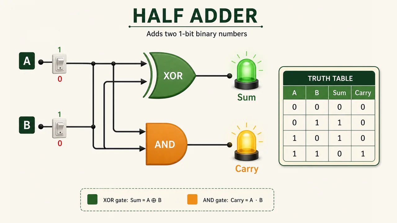
Combinational Circuits — Adders
Half Adder
A Half Adder adds two single-bit binary numbers and produces a Sum and a Carry.
| Input A | Input B | Sum (A⊕B) | Carry (A·B) |
|---|---|---|---|
| 0 | 0 | 0 | 0 |
| 0 | 1 | 1 | 0 |
| 1 | 0 | 1 | 0 |
| 1 | 1 | 0 | 1 |
- Sum = XOR gate (A ⊕ B)
- Carry = AND gate (A · B)
Full Adder
A Full Adder adds three bits — two inputs (A, B) plus a Carry-In from a previous addition. It produces a Sum and a Carry-Out.
- Built using two Half Adders and an OR gate
- Multiple Full Adders are chained together to add multi-bit binary numbers (e.g., 8-bit addition)
Sequential Circuits — Flip-Flops
A Flip-Flop is the basic memory storage element in digital circuits. It stores one bit of data (0 or 1) and retains the value until changed.
| Type | Full Name | Key Feature |
|---|---|---|
| SR | Set-Reset | Two inputs (Set, Reset); invalid state when both are 1 |
| JK | JK Flip-Flop | Improved SR — no invalid state; toggles when both inputs are 1 |
| D | Data/Delay | Single data input — output follows input on clock edge |
| T | Toggle | Toggles output on each clock pulse when input is 1 |
Flip-flops are used in registers, counters, and memory units inside the CPU.
Summary Points
| Concept | Key Details |
|---|---|
| AND | Output 1 only when ALL inputs = 1 (A·B) |
| OR | Output 1 when ANY input = 1 (A+B) |
| NOT | Inverts: 0→1, 1→0 (single input, Inverter) |
| NAND | Opposite of AND — Universal Gate |
| NOR | Opposite of OR — Universal Gate |
| XOR | Output 1 when inputs are DIFFERENT (A⊕B) |
| XNOR | Output 1 when inputs are SAME (A⊙B) |
| Universal Gates | NAND and NOR — can build any other gate from them alone |
| Boolean Algebra | Math of logic (0 and 1) — George Boole |
| Commutative Law | A+B = B+A; A·B = B·A — order doesn't matter |
| Associative Law | (A+B)+C = A+(B+C) — grouping doesn't matter |
| Distributive Law | A·(B+C) = A·B + A·C |
| Identity Law | A·1 = A; A+0 = A |
| Complement Law | A·A' = 0; A+A' = 1 |
| De Morgan's 1 | (A·B)' = A' + B' — break bar, change AND to OR |
| De Morgan's 2 | (A+B)' = A' · B' — break bar, change OR to AND |
| Half Adder | 2-bit addition: Sum = XOR, Carry = AND |
| Full Adder | 3-bit addition (A, B, Carry-In): 2 Half Adders + OR gate |
| SR Flip-Flop | Set-Reset — invalid state when both inputs = 1 |
| JK Flip-Flop | Improved SR — no invalid state, toggles when both = 1 |
| D Flip-Flop | Data/Delay — output follows input on clock edge |
| T Flip-Flop | Toggle — output toggles on each clock pulse |
| Flip-Flop Use | Registers, counters, memory units in CPU |
| Bit | Single 0 or 1 — processed by gates |
Lesson Doubts
Ask questions, get expert answers